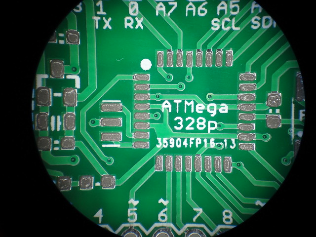
Except for the pad areas (covered here by solder paste), this board is covered by green solder mask. It's the solder mask that gives a PCB its colour. The solder mask is a little see-through, so the lighter areas are the copper tracks.
Solder mask can be applied as a dry film, or as a liquid. The fabs I use all use the liquid process.
It's standard design practice to cover vias with solder mask, because they look better that way. The problem with covered vias though, is that it's hard to use a test probe on the via to take measurements of the circuit.
If you're developing a circuit, most PCB design programs have a setting that lets you "open the vias". If you turn this on, the file that describes the solder mask will specify solder mask holes where the vias are. Each via will then have a small plated ring of solder. That way, you can easily measure signals at a via. If your design program doesn't have this setting, or you don't want to change your files between prototype and production, you can also ask me in your order email to "open the vias" of your design and I'll arrange to have it done at no cost.
All holes have a diameter, and vias, being plated holes, are no exception. Holes on my standard boards can be as fine as 0.3mm (0.012"=12mil) across. You can use 0.3mm holes with confidence. (If you have a fine pitch design, I can arrange 0.25mm or 0.2mm holes at extra cost)
Because the fabs apply the solder mask as a liquid, and because vias are usually covered, the liquid has to span the barrel of the via. For small via diameters (0.3mm) that's ok - surface tension is enough to keep the soldermask as a continuous film over the barrel. But if the barrel is wider - say 0.5mm and above - surface tension isn't enough to stop the film from popping. What happens then is one of two things. If you're lucky, surface tension turns against you and causes the liquid to pull back from the via. In this case, you'll get a via with a coppery look:

Picture supplied by M. Lövqvist, used with permission. |

Picture by Sync, used with permission. |

Picture by M. Rogger, used with permission. |
If you're unlucky though, something else happens: The barrel of the via acts as a reservoir for the solder mask liquid. This then bleeds out of the barrel and pools around the hole. This shows up as a dark blotch near the via:

It's not a good look.
So, if you want to avoid problems with solder mask over vias, you can either open your vias, or choose via diameters of 0.5mm and smaller. 0.3mm is perfectly safe.
No comments:
Post a Comment